PhotonIcs and Electromagnetics Research Symposium,
also known as Progress In Electromagnetics Research Symposium
PIERS Proceedings
Published: 2015-08-28
Self-assembled Low Density Quantum Dot and Quantum Dot-in-nanowire Structures for Quantum Photonics
By
Proceedings of 2015 Photonics & Electromagnetics Research Symposium, Prague, July 6 - 9,Page(s)315-319
Abstract
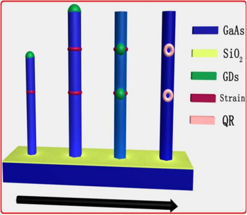
Self-assembled III-V quantum dots (QDs) are of particular attractive as solid quan- tum light emitters owing to their stability, narrow spectral linewidth, and short radiative lifetime. Meanwhile, semiconductor nanowires (NWs) have appeared as promising building blocks for fu- ture nanoscale electronic and photonic devices owing to their high crystalline quality and integra- tion possibilities. To fully explore the potential of NW systems, many investigators have turned to the synthesis of articial nanostructures in NW systems, such as quantum dots (QDs)and nanoclus- ters,to generate fascinating multifunctional properties. Single nanostructures embedded within NWs represent one of the most promising technologies for applications in quantum photonics. With NWs, a nanostructure can be constructed by inserting a slice of lower gap semiconductor along the growth direction such as CdSe/ZnSe, In(Ga)As/GaAs, GaAsP/GaAs, InAsP/InP and GaAs/AlGaAs systems, or via self-assembled epitaxy on the faceted NWs in the radial direction, utilizing the different surface energies, partly originating from different crystal lattices of hybrid materials, as a driving force. Herein, we report our latest work on self-assembled low density quantum dot and quantum dot-in-nanowire structures for quantum photonics, which might pave the way for the fabrication of highly efficient single-photon sources (SPSs) and novel quantum optics experiments. NWs samples were grown on GaAs (001) substrates sputtered with 20 nm silicon dioxide or Si (111) with native thin silicon dioxide by a Veeco Mod Gen-II Molecular Beam Epitaxy (MBE) system in traditional VLS growth mode [1–4]. The substrates were dipped for 2 s by 10% HF aqueous solution,and degased at 620◦ C for 10 min prior to growth.Growth was initiated by the condensation of a nominal 1 nm Ga in the nanocraters of the SiO2 layer. The GaAs backbones were grown at 560–600◦ C and an As2 /Ga flux ratio of 12.5–20. After depositing the GaAs backbones, the samples were exposed to a high As2 ambient overpressure to consume there maining gallium droplets on the top for preferential facet deposition. Self-assembled low density quantum dots were sandwiched between the GaAs core and GaAs/AlGaAs shell and coupled into the fundamental photonic mode of the hexagonal nanowire cavity. During the epitaxial growth on the facet of NWs backbones, a strain-driven nucleation [1] of gallium-droplets (Figure 1) leads to formation of GaAs branches [2]. Particularly for the InAs QDs embedded branched NWs, the branches were found to preferentially nucleate on the very site of quantum dot as verified by STEM energy dispersive X-ray spectroscopy (EDS) line and spot scans as shown in Figure 2. Micro-PL spectra were measured at 77 K using a continuous wave He-Ne laser for above-band excitation, which is focused on a single NW with the help of white light imaging. An enhancement of ∼ 20 times with single InAs QD signals from the branched NWs in comparison to those from the straight ones is observed (Figure 3). We attribute it to the combination of quantum confinement effect and QD-cavity interaction. For the higher band offset given by surrounding AlGaAs/GaAs thin film barriers, InAs QD exhibits a stronger confinement of excitons; while the branch helps light gathering together to the top and decreases the optical losses effectively due to its relatively large diameter, which is in consistent with numerical FDTD simulation. Sharp excitonic emission is observed at 4.2 K with aline width of 101 µeV and a vanishing two-photon emission probability of g 2 (0) = 0.031(2) (Figure 4). The branched GaAs nanowires turn out to be a better cavity to enhance the extraction efficiency of single InAs QDs emission. As the most commonly used detectors in single photon characterization, silicon avalanche pho- todiodes present the best detection efficiency at ∼ 700–800 nm. To accommodate this detecting 316 PIERS Proceedings, Guangzhou, China, August 25–28, 2014
Citation
Xiangjun Shang, Zhichuan Niu, Hai-Qiao Ni, Li-Juan Wang, Si-Hang Wei, Jian-Xing Xu, Ying Yu, and Guo-Wei Zha, "Self-assembled Low Density Quantum Dot and Quantum Dot-in-nanowire Structures for Quantum Photonics," Proceedings of 2015 Photonics & Electromagnetics Research Symposium, Prague, July 6 - 9,Page(s)315-319
References