Proceedings of 2015 Photonics & Electromagnetics Research Symposium, Prague, July 6 - 9,Page(s)329-332
Abstract
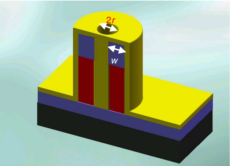
Plasmonic nano-cavity laser based on a III-V semiconductor nano-ring on silicon
can operate either in in-plane dipole mode or vertical coaxial mode. This paper gives the simula-
tion, design and some fabrication discussions of this unique nano-cavity laser. Body-of-revolution
finite-difference-time-domain (BOR-FDTD) is used for the modal analysis and design of cavity.
The spatial and temporal lasing performance of this nano-cavity laser is simulated incorporat-
ing the BOR-FDTD with multilevel gain medium model. Comparison between these two lasing
modes is presented and numerical analysis shows that the in-plane dipole mode can achieve the
smallest mode volume reported so far. Fabrication of this semiconductor plasmonic nano-cavity
laser is discussed.This semiconductor plasmonic nano-cavity laser has a deep sub-wavelength foot-
print and ultralow power consumption, which can act as an on-chip light source for intrachip data
interconnect.
Citation
Chee Wei Lee,
Kim Peng Lim,
and
Qian Wang,
"Semiconductor Plasmonic Nano-cavity Laser on Silicon: Simulation, Design and Fabrication," Proceedings of 2015 Photonics & Electromagnetics Research Symposium, Prague, July 6 - 9,Page(s)329-332